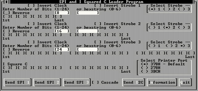
Parallel is a DOS program that uses the parallel port on the computer to program serial I2C and SPI devices such as PLL chips and other devices that require serial clock and data. The program is completely generic and can provide any arbitrary serial data stream up to 72 bits long. Clock and enable lines are provided and the user can select the polarity of each independently. The input screen is shown below.
This program can be used to program most Serial Peripheral Interface (SPI) devices such as the Motorola MC145170 IC, the MACOM MLS9300, the LMX2330 PLL chip, and many others. However only a small portion of the I Squared C (I2C) interface is implemented. The I2C portion of the program will do single byte writes to the Philips PCF8574 IC, and similar chips, but will not do data reads. Parallel port pin definitions on the PC for LPT1 are as follows.
Pin 1 = -Strobe from PC(not the strobe on main menu)
Pin 2 = +Data bit 0 from PC
Pin 3 = +Data bit 1 from PC
Pin 4 = +Data bit 2 from PC
Pin 5 = +Data bit 3 from PC
Pin 6 = +Data bit 4 from PC
Pin 7 = +Data bit 5 from PC
Pin 8 = +Data bit 6 from PC
Pin 9 = +Data bit 7 from PC
Pin 10 = -Acknowledge to PC
Pin 11 = +Busy to PC
Pin 12 = +P.End (out of paper) to PC
Pin 13 = +Select to PC
Pin 14 = -AutoFeed from PC
Pin 15 = -Error to PC
Pin 16 = -Initialize Printer from PC
Pin 17 = -Select Input from PC
Pin 18-25 = Ground
This program uses only pins 2-9, 25 as follows:
Pin 2 is Data Bit 0 used for SPI data line.
Pin 3 is Data Bit 1 used for SPI clock line.
Pin 4 is Data Bit 2 used for I2C data line.
Pin 5 is Data Bit 3 used for I2C clock line.
Pin 7 is Data Bit 5 used for SPI Strobe 1 line.
Pin 8 is Data Bit 6 used for SPI Strobe 2 line.
Pin 9 is Data Bit 7 used for SPI Strobe 3 line.
Pin 25 is ground.
A 1K resistor should be in series with the IC2 data and clock lines (pins 4 and 5) because the IC2 receive device has the capability of transmitting back since I2C is bidirectional. For SPI control, the strobe goes low, the data bit is Āplaced on the serial data line, and the clock goes high and then low while the data is valid. After all data has been clocked out, the strobe line is set high. An x in the check block indicates that the data bit Āis high. There is a special function called CASCADE that cascades the bits for SPI 1, 2, and 3 and sends it all in a continuous data stream. The enable line used for this cascaded stream is the enable line normally used for SPI 1. For the I Squared C mode, the simpliest I2C condition is sent. This is ST X X X X A2 A1 A0 0 A D0 D1 D2 D3 D4 D5 D6 D7 SP. The ST is a start condition indicated by a high to low transition of the data line while the clock line is high. The next 8 bits can be changed in the menu. The 0 following A0 signifies a write condition. Then an acknowledgement follows from the slave device. This acknowledgement must be clocked on the clock bus. Then another 8 data bits are transmitted. End of transmission is then signified by a low to high transition of the data line while the clock is high.
send email to ĀMike Ellis
You are visitor number
![]()