
| More Tutorials |
Get the complete article on mixers from Amazon on Kindle. (updated Sept. 2015)
Using Mixers in Radio Communications
By Michael Ellis
© 1999, All Rights Reserved
The Linear Diode Detector for AM Demodulation
An ideal diode conducts only during alternate half cycles of the input signal, and during the conducting half cycles the output current is proportional to the input voltage. An AM signal, applied to a diode detector as shown in figure 1, reproduce the modulating (audio) signal by mixing the AM sidebands with the AM carrier. It may be seen from figure 1 that the peak amplitude of each current pulse in the output is proportional to the peak amplitude of the input voltage during that particular conducting half cycle. Thus the peak, and therefore the average, values of the output current pulses follow the amplitude of the input voltage precisely during conducting half cycles and have the same waveform as the modulation envelope. Whether the output voltage would approach the peak or average value of the input voltage depends on the type of filter used in the output. If the filter is a bypass capacitor, and the internal resistance of the rectifier is small in comparison with the load resistance, then output voltage will tend to follow the peaks of the input voltage. Thus, the capacitor, CF, charges essentially to the peak input voltage during the conducting half cycles, but there is not time for appreciable discharge through the high resistance load during the non-conducting half cycles. If the bypass capacitor is too large, the time constant of the discharge will be so large that the detector output will not be able to follow the modulation envelope when the modulation envelope decreases amplitude rapidly.
Figure 1. AM diode detector
In addition to detection, a circuit in figure 1 has been added which is called the automatic gain control (AGC). The AGC voltage is the average value of the detector output voltage since R1 and C1 act as a filter to remove the modulating signal as well as the RF from the AGC system. This AGC voltage is therefore proportional to the amplitude of the carrier in a continuous wave system and may be used to automatically control the gain of one or more RF amplifier stages. Thus for samll input signals the RF amplifier will have high gain, but as the magnitude of the input signal increases, the gain of the RF amplifier decreases. This effect tends to keep the detector output relatively constant and prevents overdriving the RF into the saturation or cutoff regions. AGC is effectively and easily applied to a dual-gate MOSFET in the RF stage.
The Product Detector for SSB, DSB, and CW Demodulation
A product detector is a mixer used to down convert an input signal to baseband. The term, product detector, is normally used when referring to single sideband (SSB), or double sideband (DSB) demodulation, or continuous wave (CW). Essentially, it is a detector whose output is approximately equal to the product of the beat-frequency oscillator (BFO) and the RF signals applied to it. Output from the product detector is at audio frequency. Some RF filtering may be necessart at the detector output to prevent unwanted IF or BFO voltage from reaching the audio amplifier which follows the detector. In figure 2, a product detector is used to demodulate a SSB signal. The lowpass filter that follows the mixer passes only the down conversion, or difference, frequency band. Since the SSB, or DSB, signal is transmitted with no carrier, or with a supressed carrier, the frequency of the re-injected carrier in figure 2 will not be exactly the same as that of the carrier that was suppressed in the generation of the SSB, or DSB, signal. If the frequency of the re-injected carrier is not sufficiently close, then the output audio will appear to have a "Donald Duck" quality as a result of all the demodulated frequencies being in error by a constant offset.
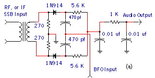
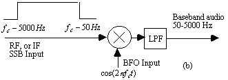
Figure 2. Product detector for demodulating a SSB, DSB, or CW signals, (a) schematic, (b) block diagram
The Quadrature Demodulator
In many modulation schemes, the carrier signal may contain both in-phase, and 90 o quadrature phase components at the carrier frequency,
wc. In the case of a simple product detector, a RF signal described by
after filtering out the double frequency component. However, if the input signal is demodulated by both an in-phase, and a quadrature, local oscillator, then the baseband output signals, I and Q, can be measured to determine the amount of in-phase, and quadrature, energy in the input signal. The quadrature modulator, demodulator, will be used as a building block in subsequent sections for more elaborate modulation and demodulation schemes.
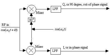
Figure 3. Quadrature demodulator recovers both the in-phase and 90 o components of the input signal
Costas Loop for Demodulating a BPSK Signal
A bipolar binary phase-shift-keyed signal (BPSK) is generated from a carrier signal,
wc, that is modulated by shifting its phase by 0 o or 180 o at a specified baud rate. A simple mixer, or ordinary phase-locked loop cannot be used to recover the binary information since there are no spectral line components at ± wc. However, since the BPSK signal has a spectrum that is symmetrical with respect to the (suppressed) carrier frequency, a special type of phase-locked loop, called a Costas loop, may be used to supply the coherent reference signal for product detection. A Costas loop for BSPK demodulation is shown in figure 4.The Costas loop is analyzed by assuming that the VCO is locked to the input suppressed carrier frequency,
wc, with a constant phase error ofThe Costas loop has a 180 o phase ambiguity. Whenever the loop is energized, it is just as likely to phase lock so that the binary 1's come out as binary 0's, and vice versa. One of two methods can be used to resolve this 180 o phase ambiguity. A known test signal could be sent over the system after the loop is turned on so that the sense of the polarity can be determined, or differential coding and deconding may be used.
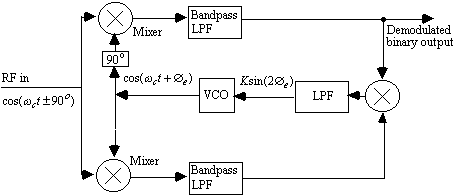
Figure 4. Costas loop for BPSK demodulation
Costas Loop for Demodulating a QPSK Signal
In quadrature phase-shift-keying (QPSK), the carrier signal can have one of four posssible phases. Independent binary messages x(t) and y(t) modulate the two quadrature components of the carrier so that the transmitted signal can be represented as
After the usual multiplications and trigonometric identities, the low frequency output of the Costas loop will be
where ![]() and sgn( ) is the hard limiting operation.
and sgn( ) is the hard limiting operation.
If the message waveforms are rectangular, the average dc outputs can be calculated as
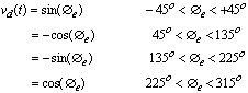
This characteristic is illustrated by the sawtooth in figure 6.
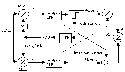
Figure 5. Costas loop for QPSK 4-phase demodulation
If the bandwidth is limited, the modulating pulses, x(t) and y(t), cannot be rectangular and the edges of the sawtooth in figure 5 are rounded. Calculations are very difficult for rounded pulses since the pulse spectrums overlap in narrowband transmission. Noise will also cause rounding of the edges of the sawtooth.
A stable lock can be achieved at any of four different phases: 0, ± 90, or 180 o . There is an inherent fourfold ambiguity that must be resolved by other means.
The limiters shown in figure 5 are essential for the correct operation of the circuit. If linear amplifiers were substituted for the limiters, the Costas loop would fail to lock.
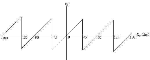
Figure 6. Phase detector characteristics of QPSK Costal loop
The Filter Method of SSB Generation
The double balanced modulator with two inputs at frequencies
wc and wm, respectively, produces an output with frequencies wc + wm and wc - wm, neglecting carrier feedthrough, local oscillator leakage, and harmonic generation. Often it is required to reject either the sum, or the difference frequency, at the output. The filter method, phasing method, or the Weaver method can be used to eliminate the unwanted product.Figure 7 shows the filter method in single sideband generation. The unwanted sideband is removed with a high Q crystal bandpass filter. A major disadvantage to the filter method is that the filter is fixed-tuned to one frequency and must have an unrealistic sharp cutoff frequency to discriminate against the unwanted sideband. Assuming a 10 MHz carrier modulated by a 50 - 5000 Hz audio signal, a 13th order elliptic bandpass filter is required with crystal Q's as high as 768,019 for 0.1 dB passband ripple, and 60 dB rejection of the unwanted sideband.
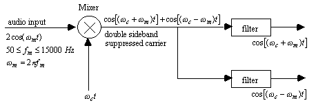
Figure 7. Filter method of single sideband (SSB) generation.
The Phasing Method of SSB Generation
The phasing method, shown in figure 8, uses a Hilbert transformer to produce a constant 90 degree phase shift over a band of frequencies. The delay block matches the delay corresponding to the delay in the Hilbert transformer. In practice, a Hilbert transformer is approximated by a phase difference network in which the two outputs of the phase-difference network track each other over a band of frequencies with a constant 90 o phase shift with unity gain at all frequencies.
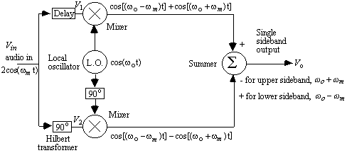
Figure 8. Phasing method of single sideband generation
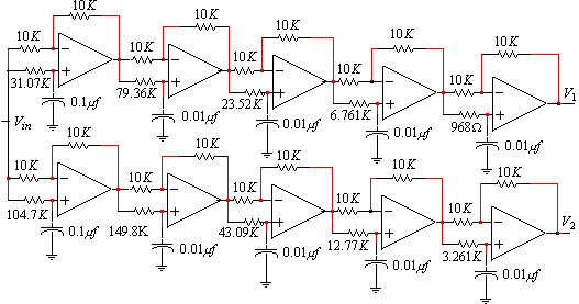
Figure 9. An active 90 o phase splitter network for figure 8
Figure 9 shows a phase difference network in which the two outputs are 90 o apart over the frequency range of 50 - 5000 Hz, with a phase error of ±0.0607 o , resulting in a rejection of 65.5 dB for the unwanted sideband. In practice, such tolerances cannot be realized even with precision components and image rejecting mixers, based on this technique, usually do not realize more than 35 dB of rejection of the unwanted sideband.
The Weaver Method of SSB Generation
The Weaver method of single sideband generation in figure 10 is similar to the phase method except that the audio broadband 90 o phase difference is implement with a quadrature mixing processing. The frequency,
w1, must be greater than the highest audio frequency, wm, and the lowpass filter is required to block the sum frequency, w1 + wm. Although an accurate broadband 90 o phase difference is not required, the two lowpass filters must closely track each other in amplitude and phase for adequate rejection of the unwanted sideband.The circuit in figure 11 shows a technique for producing a broadband 90 o (quadrature) phase shift for the local oscillator (L.O.). A phase locked loop (PLL) with an integrating loop filter will maintain 90 o phase accuracy. An integrating PLL will maintain a quadrature phase relationship when the loop is closed, however PLL circuits tend to be noisy. Sideband noise is troublesome in both SSB and FM sytems, but SSB is less sensitive to phase noise problems in the L.O.
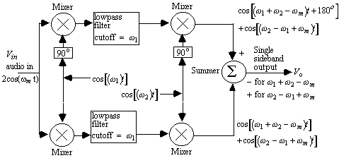
Figure 10. The Weaver method of single sideband generation
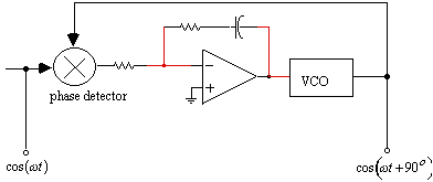
Figure 11. PLL quadrature synthesis
The Filter Method of Image Rejection
A typical AM superheterodyne radio uses an intermediate frequency (IF) of 455 Khz. If an AM station is transmiting on 1490 Khz, then the local oscillator must be tuned to 1490 + 455 Khz, or 1945 Khz, in order to convert the station frequency of 1490 Khz to the IF frequency of 455 Khz. However a station transmitting on 2400 Khz will also be converted to the IF frequency of 455 Khz unless a preselection filter is used to prevent the 2400 Khz signal from reaching the input of the mixer. The 2400 Khz station is referred to as the image.
Traditionally, a tuned filter is used at the input of the mixer to reject the image frequency (figure 12). In AM and FM radios, the front end tuned filter is designed to track the local oscillator (L.O.) by a constant difference of 455 Khz (or 10.7 Mhz in FM radios). This is usually done by a specially designed double ganged variable capacitor that sets both the frequency of the L.O. and the passband frequency of the front end filter simultaneously.
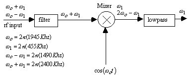
Figure 12. Filter method of image rejection.
The Phasing Method of Image Rejection
In the analysis of the phasing method in figure 13, V1 consists of a cos(
w 1t) term from the upper image and a cos(w1t) from the lower image. V2 consists of a cos[(w1t)-90o] term from the upper image and acos[(-
w1t)-90 o ] term from the lower image. A property of the Hilbert transform is that it shifts all positive frequencies by +90 o and all negative frequencies by -90 o . Therefore, the two terms, after the Hilbert transform, become cos(w1t) from the upper image, and cos[(-w1t)-180 o ] for the lower image. Since cos(A) = cos(-A), the cos[(-w1t)-180o] term is the same as cos[(w1t)+180 o ]. Adding, or subtracting, in the summer can then select whether the IF frequency, w1, is derived from the upper, or the lower, RF image. The 90 o phase difference network of figure 9 could be used to realize the Hilbert transform in figure 13, by separating the inputs to the two sections in figure 9, so that V1 and V2 are not shorted together. Figure 14 shows an alternate implementation of a 90 o phase difference network based primarily on resistors and capacitors. The ARRL handbook (1) recommends all resistors 12K, with C1 = 0.044 ![]() F, C2 = 0.033
F, C2 = 0.033 ![]() F, C3 = 0.02
F, C3 = 0.02 ![]() F, C4 = 0.01
F, C4 = 0.01 ![]() F, C5 = 5600 pF, and C6 = 4700 pF for 60 dB of sideband suppression over the range of 300 to 3000 Hz. It is important that all resistors and capacitors be closely matched for good performance.
F, C5 = 5600 pF, and C6 = 4700 pF for 60 dB of sideband suppression over the range of 300 to 3000 Hz. It is important that all resistors and capacitors be closely matched for good performance.
The values for RiCi for figure 16 are calculated using elliptic functions.Typically the worst case suppression is desired to be the highest possible. This requires an equal ripple, or Tcheybscheff approximatin. The mathematics are straightforward and given in detail by Saraga(2). For an upper and lower frequency of fu and fl respectively, the RiCi values for an n-section network are
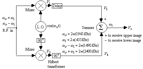
Figure 13. Phasing method of image rejection
![]()
where
![]()
is the complete elliptic integral of the first kind, and dn(u,k) is a Jacobi elliptic function
with R1-C1 defining section 1, and so on. Based on the previous equations, table 1 gives the optimal Tchebyscheff values for the R-C phasing network, fl and fu are the lower and upper frequencies, n is the number of sections, and fi, where i is 1 through n, are the frequencies of exact 90 o phase shift. The corresponding R-C values are 1/(2πfl). Sup is the minimum sideband suppression over the network range in dB. The network sections are ordered from the largest RC value to the smallest.
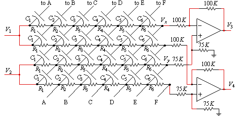
Figure 14. Six section RC 90 o phase difference network
Table 1
R-C values for 90 o phase shift network
|
fl |
fu |
n |
Sup-dB |
f1 |
f2 |
f3 |
f4 |
f5 |
f6 |
f7 |
f8 |
|
300 |
3000 |
4 |
40.5 |
332.2 |
629.8 |
1429.0 |
2709.0 |
||||
|
300 |
3000 |
5 |
52.1 |
320.5 |
500.7 |
948.7 |
1797.6 |
2808.1 |
|||
|
300 |
3000 |
6 |
63.7 |
314.2 |
435.5 |
720.3 |
1249.5 |
2066.8 |
2864.5 |
||
|
300 |
3000 |
7 |
75.4 |
310.4 |
397.8 |
595.3 |
948.7 |
1511.8 |
2262.4 |
2899.4 |
|
|
300 |
3000 |
8 |
87.0 |
308.0 |
374.0 |
519.4 |
771.2 |
1167.0 |
1732.7 |
2406.2 |
2922.5 |
|
200 |
4000 |
5 |
42.9 |
219.5 |
398.4 |
894.4 |
2008.1 |
3645.0 |
|||
|
200 |
4000 |
6 |
52.7 |
213.5 |
332.1 |
633.1 |
1263.6 |
2408.9 |
3747.8 |
||
|
200 |
4000 |
7 |
62.5 |
209.9 |
294.6 |
497.5 |
894.4 |
1608.2 |
2715.5 |
3812.0 |
|
|
200 |
4000 |
8 |
72.2 |
207.5 |
271.2 |
417.8 |
689.9 |
1159.6 |
1915.0 |
2949.6 |
3854.8 |
|
150 |
6000 |
6 |
44.7 |
163.6 |
287.7 |
628.9 |
1431.1 |
3128.3 |
5500.9 |
||
|
150 |
6000 |
7 |
53.1 |
160.0 |
247.7 |
471.0 |
948.7 |
1910.7 |
3633.0 |
5626.4 |
|
|
150 |
6000 |
8 |
61.5 |
157.6 |
223.1 |
381.3 |
696.7 |
1291.9 |
2360.2 |
4033.2 |
5710.4 |
One last comment is needed on the design of the operational amplifier circuit shown in figure 14. The input impedance at Vy is 150K. The current drawn toward the inverting input from Vx is
![]()
and since Vx = -Vy with perfect phasing, the impedance seen at Vx in the direction of the operational amplifier is 150K. Making all four resistors of equal value would reduce the sideband suppression to about 35 dB.
The Weaver Method of Image Rejection
The Weaver method of image rejection is summarized in figure 15.
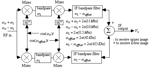
Figure 15. The Weaver method of image rejection
(1) The ARRL Handbook for Radio Amateur, (American Radio Relay League, Newington, 1993), and many previous editions.
(2) Saraga, W., "The Design of Wide-Band Phase Splitting Neworks," Proc IRE, Vol 38, p 754 (1950)
(3) Cayley, A., An Elementary Treatise on Elliptic Functions, (Bover, New York, 1961).
(4) Abramowitz, M., and Stegun, I., Handbook of Mathematical Functions with Formulas, Graphs, and Mathematical Tables, National Bureau of Standards, Applied Mathematics Series, (US Government Printing Office, Washington, DC 1964
(5) Schmidt, Kevin, Phase-Shift Network Analysis and Optimization
(6) Cracknell, A.P., Applied Group Theory, (Pergaman, Oxford, 1968)
You are visitor number
![]()