| More Tutorials |
Get the complete article on mixers, including Gilbert cells on Kindle from Amazon. (updated Sept. 2015)
Gilbert Cells
A Gilbert cell is a cross-coupled differential amplifier, similar to the topology in figure 1, where the gain is controlled by modulating the emitter bias current. The amplitude of a differential input RF signal, applied to pins 6 and 7 of the HFA3101, can be linearly controlled by a differential ac voltage applied to pins 1 and 4. Because the gain control is highly linear, Gilbert cells are often referred to as four-quadrant multipliers and have common applications as mixers, AGC amplifiers, amplitude modulators, double sideband (DSB) modulators, single sideband (SSB) modulators, AM detectors, SSB and DSB detectors, frequency doublers, squaring circuits, dividers, square-root circuits, and root-mean-square, r.m.s., measuring circuits. In order to understand how the Gilbert cell operates, it is necessary to review some fundamental concepts of bipolar transistors.
Bipolar Junction Transistor Models
Figure 2 shows two equivalent small signal models for a bipolar transistor. All ac components will be represented by a lower case letter with vbe denoting the ac input voltage across the base-emitter junction of the transistor, and ic will be the corresponding ac collector current. The transconductance, gm, of a transistor is set by it's dc quiscent collector current. In figure 3, the dc quiscent collector current is denoted by Io/2, therefore
![]() (1)
(1)
where VT is the thermal voltage and is taken at 0.025 volts at room temperature.
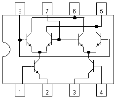
Figure 1. Harris HFA3101 5 GHz Gilbert cell array.
Once gm is established by setting the value of the dc quiscent collector current, Io/2, the gain can be derived from
gm vbe = ic = ![]() ib (2)
ib (2)
where ![]() is the current amplification of the transistor and is dependent upon the transistor selected.
is the current amplification of the transistor and is dependent upon the transistor selected.
The input impedance for an ac signal between the base-emitter junction of a transistor will be denoted by ![]() and is given by
and is given by
![]() (3)
(3)
Equations (1-9) are small signal approximations and they are valid for vbe less than 10 millivolts.
The Differential Amplifier
Figure 3 shows a differential amplifier using a constant current source. The following equations immediately provide the means to analyze figure 3. The ac voltage across the base-emitter junction of Q1 is
![]() , (4)
, (4)
or
![]() . (5)
. (5)
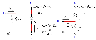
Figure 2. Equivalent small signal models for a bipolar transistor.
The ac gain from vin to vout1 is then
![]() (6)
(6)
Notice here that if Rin << than ![]() , the total gain is linearly dependent on the value of the constant current source, Io. In this case
, the total gain is linearly dependent on the value of the constant current source, Io. In this case
![]() (7)
(7)
The total voltage at vout1 is
![]() (8)
(8)
Similarly, at the collector of Q2, the output voltage, vout2 is
![]() (9)
(9)
with the assumption that both transistors are well matched.
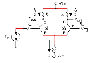
Figure 3. Differential amplifier with constant current source.
The Single Balanced Modulator
In figure 4, the concept of a differential amplifier is now extended to a single balanced modulator by modulating the constant current source with a low frequency signal such that
I = Io + k1 cos(
wmt ) for k1 < Io. (10)If vin is also represented as a sine wave such that
vin = k2 cos(wct) (11)
then
substituting equations (10) and (11) into equations (8) and (9) provide
![]() (12)
(12)
and
![]() (13)
(13)
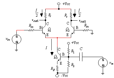
Figure 4. Single balanced modulator
It is seen that both (12) and (13) contain frequency components at four distinct frequencies, including wc, wc - wm, wc + wm, and wm. By taking the difference of vout1 and vout2 with a difference amplifier, the baseband term at frequency, wm, is eliminated leaving
![]() (14)
(14)
or, by using a trigonometric identify,
![]() (15)
(15)
The balanced modulator with the difference amplifier that implements equation (15) is shown in Figure 5. The corresponding voltages as seen on an oscilloscope for vout1, vout2, and vout are shown in Figure 6.
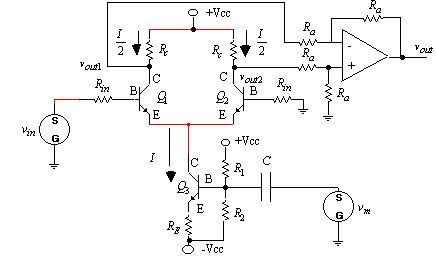
Figure 5. Single balanced modulator with difference amplifier
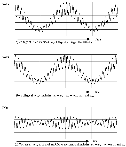
Figure 6. Voltages at vout1, vout2, and vout, for a single balanced modulator with difference amplifier
The Double Balanced Modulator
The double balanced modulator eliminates the carrier frequency at
wc and effectively implements a mixer that generates only the sum and difference frequencies. An extension of the balanced modulator to create a double balanced modulator is shown in figure 7. By analogy with the balanced modulator, using equations (12) and (13), the equations for the double balanced modulator in figure 7 become (16)
(16)
and
![]() (17)
(17)
The difference amplifier at the output of figure 7 eliminates the dc term leaving
![]() (18)
(18)
The output waveform, vout, for the double balanced modulator is shown in figure 8.
The double balanced mixer in figure 9 generates both a sum and difference frequency. Further deriviatives of the double balanced mixer can be used to generate only the upper, or lower, sideband during the modulation process, or can be used to mix two signal and reject either the lower, or the upper, image frequency. The analysis details are based on the trigonometric identity
![]() (19)
(19)
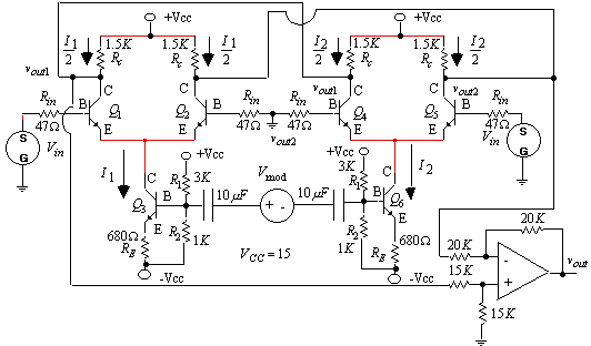
Figure 7. Double balanced modulator with elimination of the dc component at vout

Figure 8. Typical output waveform for a double balanced modulator shows a double sideband (DSB) waveform and includes only the sum and difference frequencies, ![]() .
.
Copyright 1999, Mike Ellis