RF Directional Couplers
Copyright by Michael G. Ellis, Ph.D.
Electronic System Products
A division of ANTEC
| More Tutorials |
The equations that describe the performance of transformer based directional couplers are derived. The best theoretical performance available from a directional coupler, using ideal transformers, is a function of the turns ratio, and the terminating impedances. At VHF and UHF frequencies, wire gauge and core material can be chosen to closely approximate the response based on the solution of these equations. A computer program is presented as a design aid.
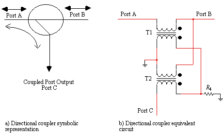
A directional coupler separates signals based on the direction of signal propagation. These devices are used to unequally split the signal flowing in the mainline and to fully pass the signal flowing in the opposite direction. In an ideal situation some portion of the signal flowing into port A will appear at Port C. Likewise any signal flowing into port C will be coupled fully to port A. However ports B and C are isolated in that any signal flowing into port B will not appear at port C but will feed through to port A. The generic RF directional coupler symbol, shown in Figure 1(a), is usually realized by two transformers connected as shown in Figure 1(b). Directional couplers of
Figure 1. Directional coupler circuit configurations
this type are impedanceless, in that they become 50 ohm , or 75 ohm , directional couplers simply by matching all ports to either 50 ohms , or 75 ohms , respectively.
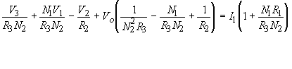
Figure 2 is a generic model for analysis. In the forward mode of operation, V1 is the applied input voltage with V2, V3, and V4 replaced by shorts. Vo then becomes the output voltage. A portion of the output voltage, Vo, is coupled to R3, and ideally no voltage appears across R4. In the reverse mode of operation, V2 is the applied input voltage with V1, V3, and V4 replaced by shorts. The output voltage then becomes the voltage across R1. A portion of the output voltage (voltage across R1) is coupled to R4, and ideally no voltage appears across R3. The turns ratio of T1 is 1:N1 where N1 is the secondary of the transformer T1. Similarly, the turns ratio of T2 is 1:N2 where N2 is the secondary of the transformer T2. The location of the dots beside the transformers denote that the voltage across the primary is in phase with the voltage across the secondary. Voltage sources are shown at all four ports because, by shorting each of the three voltages sources to ground, the input impedance of the port with the non-zero voltage source can be found from the nodal equations.

Figure 2. Nodal voltages and currents in a directional coupler
The equations shown in Figure 2 can be written down by inspection using ohm's law and Kirchhoff's voltage and current laws.
1. I1 is defined to be the current through R1.
2. The voltage across the primary of T1 is defined to be VL.
3. The voltage at Node 1 is defined to be Vo.
4. The current flowing through R2 is therefore the voltage across R2, divided by
R2, or (Vo-V2)/R2.
5. The voltage across the secondary of T1 is N1 times the voltage across the
primary of T1, or N1VL.
6. If the current through the primary of T1 is I1, then the current through the
secondary of T1 has to be I1/N1.
7. The voltage across the secondary of T2 has already been denoted as Vo.
8. Therefore the voltage across the primary of T2 has to be Vo/N2.
9. The current through R3 has to be the sum of the voltages across R3 divided
by R3. These three voltages are V3, Vo/N2, and N1VL and they add since
they are all in phase. (If the solution to the equations shows otherwise, then
one of the currents will simply be negative indicating that it actually flows
in the opposite direction than initially assumed.) The current through R3
becomes V3/R3 + Vo/(N2R3) + N1VL/R3.
10. The current through the secondary of T2 has to be equal to the current through
R3 divided by N2, or V3/(R3N2) + Vo/(N2N2R3) + N1VL/(R3N2).
11. The current through R4 is equal to the voltage across R4, divided by R4. The
voltages to the left and right of R4 are N1VL and V4, respectively. They add
since they are in phase. Therefore the current through R4 is N1VL/R4+V4/R4.
Now the current flowing into Node 1 has to be equal to the currents flowing out of Node 1, therefore
![]() (1)
(1)
Also the currents flowing into Node 2 have to be equal to the current flowing out of Node 2, or,
![]() (2)
(2)
It is necessary to eliminate the variable, VL, using the equation
![]() (3)
(3)
Substituting equation (3) into (1) and (2) and rearranging terms, the final nodal equations become
![]() (4)
(4)
and
 (5)
(5)
Equations (4) and (5) are easily solved for Vo and I1 since V1, V2, V3, and V4 are known and only one is non-zero for a given analysis. From inspection of Figure 2, the input impedances at each port are given by
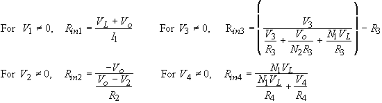 (6)
(6)
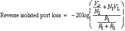
The return loss, RL, at port x (for x = 1,2,3, or 4) is given by
![]() (7)
(7)
In the forward direction (V1 not equal to 0), from inspection of Figure 2 the loss at the various ports is given by
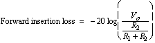 (8)
(8)
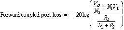 (9)
(9)
 (10)
(10)
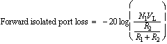
In the reverse direction (V2 not equal to 0), the loss at the various ports are given by
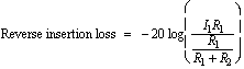 (11)
(11)
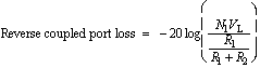 (12)
(12)
 (13)
(13)
Table 1 summarizes a portion of the design data that is available from the computer program based on the preceding equations. The return loss values in Table 1 are valid for any arbitrary characteristic impedance, Zo; therefore Table 1 can be used to design both 50 ohm and 75 ohm directional couplers. A turns ratio of 1.5 is achieved by 2 turns of wire on the primary, and 3 turns of wire on the secondary. Notice that the coupled port loss is very closely approximated by the equation
![]() (14)
(14)
The range of toroidal based directional couplers can span two decades of frequency and commonly covers the frequency range of 5 MHz to 1 GHz.
Table 1
Directional coupler loss as a function of turns ratio
| N1 | N2 | Insertion
Loss |
Coupled
Port Loss |
Input
Return Loss |
Output
Return Loss |
Coupled Port
Return Loss |
| 1.0 | 1.0 | 7.96 dB | 1.94 dB | 14.0 dB | 14.0 dB | 14.0 dB |
| 1.5 | 1.5 | 2.60 dB | 3.94 dB | 15.7 dB | 15.7 dB | 15.7 dB |
| 2.0 | 2.0 | 1.29 dB | 6.15 dB | 19.4 dB | 19.4 dB | 19.4 dB |
| 2.5 | 2.5 | 0.78 dB | 8.01 dB | 22.7 dB | 22.7 dB | 22.7 dB |
| 2.5 | 3.0 | 0.65 dB | 8.76 dB | 26.1 dB | 22.6 dB | 22.6 dB |
| 3.0 | 2.5 | 0.65 dB | 8.76 dB | 22.6 dB | 26.1 dB | 26.1 dB |
| 3.0 | 3.0 | 0.52 dB | 9.57 dB | 25.6 dB | 25.6 dB | 25.6 dB |
| 3.0 | 3.5 | 0.45 dB | 10.2 dB | 28.4 dB | 25.6 dB | 25.6 dB |
| 3.5 | 3.0 | 0.44 dB | 10.2 dB | 25.6 dB | 28.4 dB | 28.4 dB |
| 3.5 | 3.5 | 0.38 dB | 10.9 dB | 28.2 dB | 28.2 dB | 28.2 dB |
| 3.5 | 4.0 | 0.33 dB | 11.5 dB | 30.6 dB | 28.2 dB | 28.2 dB |
| 4.0 | 3.5 | 0.33 dB | 11.5 dB | 28.2 dB | 30.6 dB | 30.6 dB |
| 4.0 | 4.0 | 0.28 dB | 12.1 dB | 30.4 dB | 30.4 dB | 30.4 dB |
| 4.0 | 5.0 | 0.23 dB | 13.0 dB | 34.6 dB | 30.5 dB | 30.5 dB |
| 5.0 | 4.0 | 0.23 dB | 13.0 dB | 30.5 dB | 34.6 dB | 34.6 dB |
| 5.0 | 5.0 | 0.18 dB | 14.0 dB | 34.2 dB | 34.2 dB | 34.2 dB |
| 5.0 | 6.0 | 0.15 dB | 14.7 dB | 37.5 dB | 34.2 dB | 34.2 dB |
| 6.0 | 5.0 | 0.15 dB | 14.7 dB | 34.2 dB | 37.5 dB | 37.5 dB |
| 6.0 | 6.0 | 0.12 dB | 15.6 dB | 37.3 dB | 37.3 dB | 37.3 dB |
| 6.0 | 7.0 | 0.11 dB | 16.2 dB | 40.1 dB | 37.3 dB | 37.3 dB |
| 7.0 | 6.0 | 0.11 dB | 16.2 dB | 37.3 dB | 40.1 dB | 40.1 dB |
| 7.0 | 7.0 | 0.09 dB | 16.9 dB | 39.9 dB | 39.9 dB | 39.9 dB |
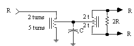
Figure 3. Transformer-type 3.5 dB power splitter. R = 75 for a 75 ohm system.
As the turns ratio of T1 and T2 approach N1 = 1 and N2 = 1, the directional coupler does not degenerate into a 3 dB splitter. If a coupled port loss of 3.5 dB - 5 dB is desired, the splitter configuration shown in Figure 3 should be used. This basic splitter achieves 3.5 dB loss on each port. A resistive pi-pad on the output port defined as the coupled port can give an additional 0-1.5 dB, or more, attenuation. The capacitor, C, is typically on the order of 1 pF and improves return loss.
The ferrite binocular in Figure 4 can be used to realize both the T1 and T2 transformers on a single twin hole ferrite core. Low frequency response is dictated by the ferrite material characteristics. High frequency response is partially governed by total wire length, since the core effects are no longer dominant near the high frequency end (2). Interwinding capacitance, leakage inductance, copper losses and transformer coupling below unity (k <1) also degrade high-end performance. Small shunt capacitances to ground at the coupler ports can be used to improve match and directivity at the expense of bandwidth. At higher frequencies, lead length must be kept to a minimum to limit parasitic inductance. To achieve broadband performance, ground connection lengths must be minimized.
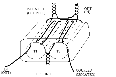
Figure 4. A 10 dB directional coupler.
Increasing the number of turns on the primary is limited by the number of wires that can fit through the core. For Figure 4, a turns ratio of 6:2, instead or 3:1, can give superior results for a given frequency range. (The number of turns is determined by the number of times that the wire is threaded through the center of the core even though it may not make a complete 360 degree turn.) High frequency response increases as core size and wire diameter decrease.
The response of the directional coupler can vary dramatically depending on the interleaving of the primary and the secondary coils. If possible, intersperse the secondary windings with turns from the primary. Designers will often set the spacings of the primary and secondary coils to optimize certain design parameters. The insertion loss at high frequencies can be decreased in the main path at the expense of high frequency response on the coupled port by loosely coupling the primary and the secondary coils of T2 so that less high frequency energy is coupled to the coupled port. Changing the diameter of the primary wire relative to the secondary changes the coupling by tenths of a dB (3). Using heavier gauge magnet wire for the primaries reduces mainline insertion loss and improves power-handling capability. The isolated port should connect to a good Zo ohm load impedance, such as a small chip resistor. A small capacitor in the range of 0.5 - 2 pF can be connected in parallel with this resistor to improve directivity.
A response typical for the coupled port is shown in Figure 5 using a Fair-Rite core and magnet wire. The coupled port frequency response is flat within ±0.5 dB from less than 50 MHz to 900 MHz.
McWhorter provides other examples using different materials (2). A 10 dB coupler was fabricated on a Siemens B62152-A0008-X030 core. Each primary consisted of one turn of #33 magnet wire. Each secondary consisted of three turns of #38 magnet wire. This coupler was used in a CW environment with excellent performance in the 10-1000 MHz band.
Two Micrometals T25-0 phenolic toroids were used to create a 20 dB coupler for use in the 500-2200 MHz band. Each primary consisted of one turn of #32 silver-coated Teflon-insulated magnet wire. Each secondary consisted of 10 turns of #36 Formvar-coated magnet wire.
A computer program is presented as an aid in designing transformer based directional couplers. It is provided in a DOS BASIC version (with source), a DOS Visual Basic version, and in a Windows Visual Basic version. The program solves the equations derived in this article for arbitrary termination impedances and arbitrary turns ratios. A sample output screen is given in Figure 6 for a directional coupler terminated in 75 Ω on all ports and with a turns ratio of 5:1 for both T1 and T2.
The computer program will accept turns ratios for T1 and T2 that are greater than unity, less than unity, or negative. A turns ratio of 0.5 would indicate 2 turns on the primary for every turn of the secondary. A negative turns ratio would indicate that the user desires to reverse the polarity of the secondary of the transformer relative to the definition given in Figure 2. As can be seen from Figure 6, the return loss of a directional coupler theoretically never provides a perfect match. The total input power into the directional coupler is computed and compared to the sum of the power flowing out of the remaining three ports as a check on the accuracy of the computations.
The equations derived in this article apply equally to both the 0o and the 180o directional coupler. These couplers are shown in Figure 7. The phase of the coupled port depends only on which end of the directional coupler is defined as the input.
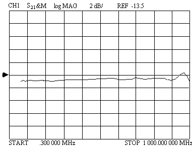
Figure 5. Typical coupled port response.
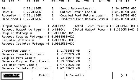
Figure 6. Sample design output screen
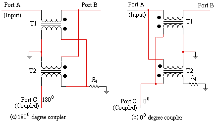
Figure 7. Definition of (a) inverting coupler, and (b) non-inverting coupler
References:
1. U.S. Patent Number 3,426,298, Broadband Directional Coupler.
2. Mark McWhorter, Broadband RF Transformer Directional Couplers, RF Design
Magazine, July 1991, pp 53-58
3. Nic Hamilton, RF Transformers Part 1: The Windings, RF Design Magazine, June
1995, pp 36-44
About the Author
Michael Ellis can be reached at Electronic System Products (ESP), 11450 Technology Circle, Duluth, GA 30097. Email at michaelgellis@hotmail.com