A Capacitor Coupled DC Power Supply for CATV Applications
Electronic System Products, Inc.
ANTEC Technology Center
by Michael G. Ellis, Ph.D.
| More Tutorials |
EDN published version.
A CATV system requires trunk amplifiers, power inserters, taps and passives, and other types of modules to be placed along the CATV path. In most cases, these modules require a dc power supply; a few will need only a modest dc voltage at a small current level. This article is a design guide for a low cost transformerless power supply that will provide a regulated voltage at low current levels directly from the CATV cable line.
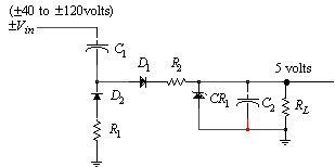
Coaxial CATV systems are powered by a 60 Hz square wave that shares the center conductor with the television channels. Active devices are often required to be placed along the distribution path. If the dc power requirements, voltage and current, are small for these active devices, then a transformerless power supply similar to the topology in Figure 1 can be used as a low cost means of providing power to the device. Although this example uses a 5 volt, 10 milliamp supply, the design equations that are derived will later be generalized for any desired output voltage and current.
Given the circuit topology in Figure 1 with the input voltage consisting of a square wave and an output load of 5 volts at 10 ma, the problem is to find the component values for the resistors and capacitors. Assume that the input voltage can range from ±40 to ±120 volts with a wave shape as shown in Figure 2.

Figure 1. Low current power supply circuit

Figure 2. Square wave input voltage, Vin. Range will be ±40 to ±120 volts.
To derive the design equations, it will be necessary to assume that C1 fully charges on each half cycle. This assumption will be validated later.
Design Derivation
Since an output voltage of 5 volts is specified, the required zener (CR1) voltage is also 5 volts.
Figure 3 shows the model to compute the voltage drop across C1 and the end of the negative half cycle. Similarly, figure 4 shows the model for computing the voltage drop across C1 and the end of the positive half cycle.
Using the relation,
Q = C1V (1)
the total charge transferred over one full cycle is
C1(2Vin-6.2) (2)
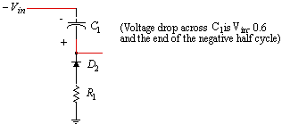
Figure 3. Voltage drop across C1 at end of negative half cycle.
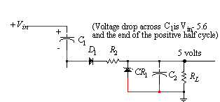
Figure 4. Voltage drop across C1 at end of positive half cycle.
But current is charge per second, so the average current flow through D1 over one second is
I=60C1(2Vin-6.2) amps (3)
since there are 60 cycles per second.
The desired maximum output current is 10 milliamps. Vin can range from ±40 to ±120 volts (square wave). Using the worst case input voltage (±40 volts), C1 can be computed from equation (3) as
![]() (4)
(4)
C2 should be large enough to hold the output voltage to within 5% of 5 volts over the negative half cycle using the maximum load of RL = 500 ohms (for 10 milliamps). Therefore
![]() (5)
(5)
or
 (6)
(6)
using 1/120 second for the time duration of the negative half cycle.
To determine R2, assume the maximum peak instantaneous power that the zener diode can handle is 10 watts. Also assume that the average power that the zener can handle is 0.2 watts. (The zener diode will have to be selected to meet these specifications.) Since the output current is already determined to be 10 milliamps, maximum, the average power to the zener with an input voltage square wave of ±40 volts is
0.01 amps *5 volts = 0.05 watts (7)
but for the maximum input voltage square wave of ±120 volts, the average power to the zener will be approximately
0.03 amps * 5 volts = 0.15 watts (8)
However the peak surge current to the zener is approximately given by
![]() (9)
(9)
since the input voltage seen by R2 is Vin plus the voltage across C1, or approximately
2 Vin total. From equation (9), for Vin = 120 volts (worst case), and an assumed surge current rating of 2 amps on the zener, the minimum value of R2 becomes 120 ohms.
There is another limiting factor on R2. From our initial assumption C1 must be fully charged in each half cycle of the input voltage, Vin. In five time constants, C1 will charge to 99.6% of its final voltage. Therefore from the time constant R2-C1, R2 may be determined from
 10)
10)
The bounds on R2 become
![]() (11)
(11)
R2 can be selected near the high end to limit the surge current to the zener, therefore we choose R2 = 680 ohms, limiting the zener surge current to 0.35 amps. For equal time constants on both the positive and negative half cycles in the input voltage, choose
R1 = R2 = 680 ohms. (12)
The maximum power dissipated in R1 and R2 occurs when Vin = ±120 volts. Then the average current is approximately 3 times higher than when Vin was ±40 volts. The average current with Vin = ±120 volts is approximately 0.03 amps. The maximum dissipated power in R1 and R2 is
![]() (13)
(13)
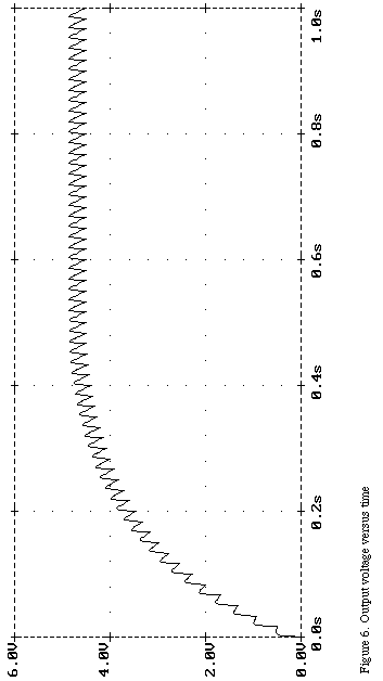
The final design for a 5 volt, 10 milliamp supply is given in Figure 5. Although it is not shown, a RF choke should be added in series with C1 as an RF block. The spice simulation plot shown in Figure 6 is plotted from the data in Table 1.
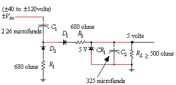
Figure 5. Final design
Table 1. Spice Simulation File
EXAMPLE - Capacitive coupled supply
.WIDTH OUT=80
.OPT ITL5=10000 ACCT NOECHO NOPAGE OPTS RELTOL=.001
.TRANS .5S 1S .001S
VPULSE 1 0 PULSE (-40V 40V 100NS 100NS 100NS .00833S .016666S)
C1 1 2 .00000225
D1 2 4 DIODE
D2 3 2 DIODE
R1 3 0 680
R2 4 5 680
R3 5 0 500
C2 5 0 .000325
D3 0 5 ZENER
.MODEL DIODE D(RS=1 VJ=0.6)
.MODEL ZENER D(RS=1 VJ=0.6 BV=5 IBV=1)
.PROBE
.END
Summary:
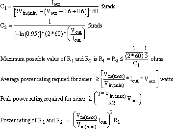
Based on the preceding example, the generalized design equations for a 60 Hz square wave ac input can be written as follows.
Input parameters:
Minimum ac square wave input voltage = Vin(min)
Maximum ac square wave input voltage = Vin(max)
Desired dc output voltage = Vout
Maximum desired dc output current = Iout
Component values:
Zener (CR1) voltage = Vout
Michael Ellis is a senior staff engineer at ANTEC/Electronic System Products and is involved in the design of CATV products. He can be reached at 11450 Technology Circle, Duluth, GA 30097
References:
Phillip E. Allen and Edgar Sanchez-Sinencio: Switched Capacitor Circuits, Van Nostrand Reinhold, New York, 1984